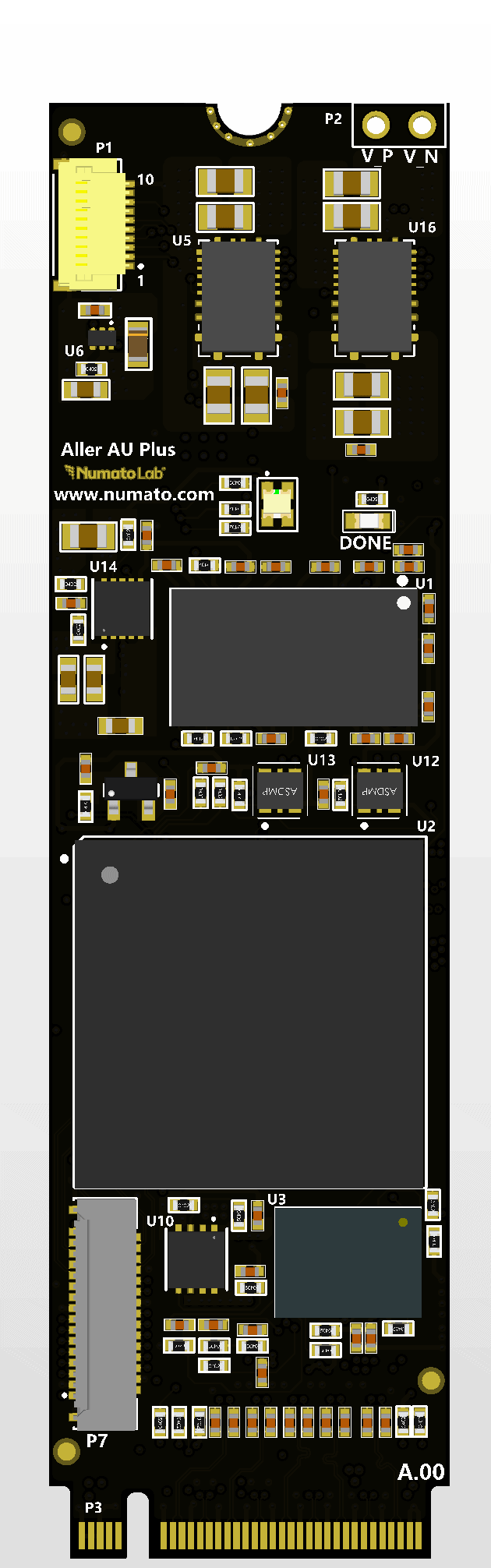
Introduction
The Aller AU-Plus FPGA Module is a high-performance development platform featuring an Artix Ultrascale+ FPGA, optimized for advanced computing and high-speed data processing. Equipped with an M.2 interface, SPI flash, DDR4 memory, and a TPM (Trusted Platform Module) for enhanced security, this board is ideal for applications requiring speed, security, and flexibility. The M.2 interface enables seamless integration with SSDs and other expansion modules, making it a versatile choice for embedded systems, data acquisition, and AI edge computing.
Board Features
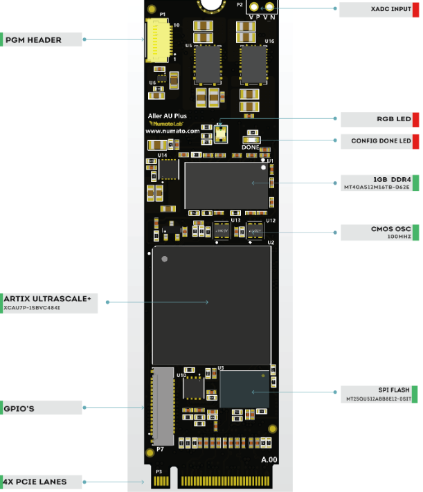
- Device: AMD Artix Ultrascale+ FPGA (XCAU7P-1SBVC484I)
- DDR4: 8Gb DDR4
- x4 lane PCIe Gen3 (8 GT/s)
- Onboard 512Mb QSPI flash memory for FPGA configuration
- FPC header for programming and debugging
- 100 MHZ CMOS oscillator
- 1 x Trusted Platform Module (AT97SC3205)
- M.2 Connector Interface, M-Key
- Powered from M.2 connector
- 1 RGB LED for custom use
Applications
- High-Speed Data Acquisition and Processing
- AI/ML Edge Computing
- Signal Processing and Analysis
- Memory Intensive FPGA development
- Secure IoT Gateways (using TPM for enhanced security)
- Network Acceleration and Traffic Management
- Product Prototype Development
- Cryptographic Applications and Secure Boot
- Storage Solutions with M.2 SSDs
How to use Aller AU-Plus FPGA Module
Hardware Accessories Required
- Aller AU-Plus FPGA Module.
- Aller AU-Plus Programmer.
Connection Diagram
This diagram should be used as a reference only. The schematics are available at the end of this document for detailed information.
Temperature and Heat Dissipation
M.2 form-factor doesn’t permit thick and large surface-area PCBs, so heat dissipation in M.2 profile modules is always a challenge. M.2 modules are traditionally used with application specific ICs for WiFi, USB etc, and the heat dissipation in those are comparatively lesser whereas in case of FPGAs, heat dissipation and power requirements are higher.
Aller features an Artix Ultrascale+ SBVC484I FPGA with -1I speed grade (-40°C~100°C range) and 3200 MT/s DDR4 RAM. When running at maximum FPGA resource utilization and DDR4 running at max 3200 MT/s, huge amount of heat is dissipated. PCB thickness and surface area being low, the junction temperature of FPGA can rise to a high value. FPGA would get damaged if junction temperature rises above 100 °Celsius.
Therefore, heat sink is mandatory when using Aller with heavy designs. Else, the FPGA and the board may get damaged. Heat sinks with good thermal coupling have been tested to decrease the temperatures by 15-20°C. If the temperature still approaches dangerous zone, then forced air cooling using fans might be required.
Aller ships with a standard heat sink which should be sufficient for most use cases. It should be noted that with the addition of heat sink, the module may not fit inside some space constrained cases such as thin laptops. For simpler designs running at lower frequency and not using DDR4, the heat dissipation is less, and heat sink is not compulsorily required. It is expected that users do their own independent power analysis using Xilinx Power Estimator to find out the optimal cooling requirements for Aller.
We recommend maintaining the junction temperature of FPGA below 70°C range. Users can use System Management Wizard block inside Artix Ultrascale+ FPGAs to measure temperature.
Power
Aller AU-Plus FPGA module requires +3.3V power supply to function properly. It takes power from M.2 connector. Current requirement for this board largely depends on your application.
DDR4
Aller AU-Plus FPGA Module uses DDR4 which is a high-speed dynamic random-access memory internally configured as an eight-bank DRAM. The DDR4 SDRAM uses an 8n-prefetch architecture to achieve high-speed operation. The 8n-prefetch architecture is combined with an interface designed to transfer two data words per clock cycle at the I/O pins. DDR4 is connected to the bank 66 of Aller AU-Plus FPGA module.
SPI FLASH
The Aller AU-Plus FPGA Module has 512 Mbit of Quad SPI flash memory. It is a serial NOR flash which operates at the voltage of 1.8 V. It serves as the default primary boot device.
Clock
Fabric Clock
Clock pins FPGA pins
REF_CLK_P K18
REF_CLK_N J18
DDR4 Reference Clock
Clock pins FPGA pins
DDR4_REFCLK_P B14
DDR4_REFCLK_P B15
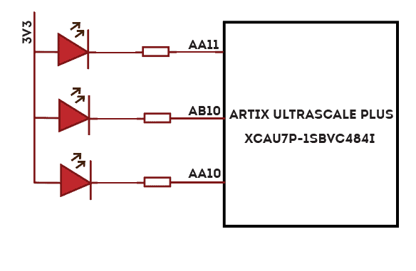
RGB LED
Aller features one RGB LED on the module which can be used for custom or debug purposes.
M.2 Edge Connector
M.2 edge-connector on Aller AU-Plus module provides the power to the board. Each lane is capable of 8GT/s resulting in maximum theoretical data transfer rate of 4GB/s for all 4 lanes combined.
M.2 pin name Signal name FPGA Pins
REFCLK_P MGTREFCLK0P_124 AA17
REFCLK_N MGTREFCLK0N_124 AA18
M2_TX0_P MGTHTXP0_124 AB19
M2_TX0_N MGTHTXN0_124 AB20
M2_TX1_P MGTHTXP1_124 Y19
M2_TX1_N MGTHTXN1_124 Y20
M2_TX2_P MGTHTXP2_124 V19
M2_TX2_N MGTHTXN2_124 V20
M2_TX3_P MGTHTXP3_124 T19
M2_TX3_N MGTHTXN3_124 T20
M2_RX0_P MGTHRXP0_124 AA21
M2_RX0_N MGTHRXN0_124 AA22
M2_RX1_P MGTHRXP1_124 W21
M2_RX1_N MGTHRXN1_124 W22
M2_RX2_P MGTHRXP2_124 U21
M2_RX2_N MGTHRXN2_124 U22
M2_RX3_P MGTHRXP3_124 R21
M2_RX3_N MGTHRXN3_124 R22
M2_PERST# IO_L6N_HDGC_84 AA6
M2_CLKREQ# IO_L7P_HDGC_84 W8
M2_WAKE# IO_L6P_HDGC_84 Y6
Trusted Platform Module(TPM)
The Trusted Platform Module(TPM) is an integrated security module for hardware authentication. The security module is used primarily for cryptographic key generation, key storage and key management as well as generation and secure storage for digital certificates.
Signal Name Signal name FPGA Pins
TPM_MOSI IO_L4N_AD12N_84 AB8
TPM_MISO IO_L4P_AD12P_84 AA8
TPM_CS# IO_L3N_AD13N_84 Y9
TPM_CLK IO_L3P_AD13P_84 Y10
TPM_RST# IO_L5P_HDGC_84 AA7
FPC header (P1)
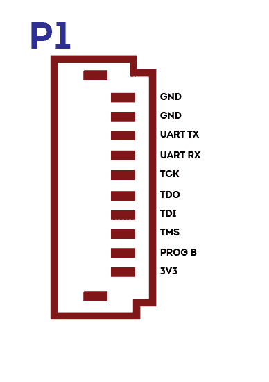
The FPC header (P1) on the Module is used for FPGA programming and includes JTAG and UART pins.
FPC header (P7)
FPC header P7 on the module is connected to the Cruvi connector on the Aller AU-Plus programmer through an FPC cable.
The table lists all the pins on the FPC header (P7).
FPC header pins CRUVI pins Signal name FPGA pins
1 RESET VCCO_104 U9
2 A5_N VCCO_104 AB2
3 B5_N GND Y1
4 A5_P GND AB3
5 B5_P HD104_IO1_P W1
6 A4_N HD104_IO2_P AB4
7 B4_N HD104_IO1_N V1
8 A4_P HD104_IO2_N AB5
9 B4_P HD104_IO3_P U2
10 A3_N HD104_IO4_P AA5
11 B3_N HD104_IO3_N AA1
12 A3_P HD104_IO4_N Y5
13 B3_P HD104_IO5_P AA2
14 GND HD104_IO6_P
15 GND HD104_IO5_N
16 A2_N HD104_IO6_N V5
17 B2_N GND V4
18 A2_P GND U5
19 B2_P HD104_IO7_P U4
20 A1_N HD104_IO8_P Y4
21 B1_N HD104_IO7_N V2
22 A1_P HD104_IO8_N W4
23 B1_P HD104_IO9_P U3
24 A0_N HD104_IO10_P AA3
25 B0_N HD104_IO9_N W2
26 A0_P HD104_IO10_N Y3
27 B0_P HD104_IO11_P W3
28 GND HD104_IO12_P
29 GND HD104_IO11_N
30 VCCO_104 HD104_IO12_N
31 VCCO_104 HD_IO
Generating Bitstream for Aller AU-Plus FPGA Module
The bitstream can be generated for Aller AU-Plus FPGA Module in Vivado by following the steps below:
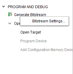
Step 1: It is recommended to generate .bin bitstream file along with .bit bitstream file. Right Click on “Bitstream Settings”.
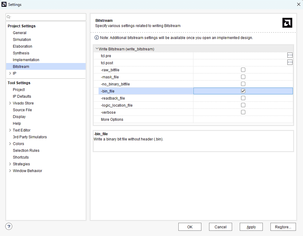
Step 2: Select “-bin_file*” option in the dialog window and Click “OK”.
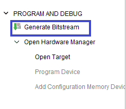
Step 3: Finally click “Generate Bitstream”.
Programming Aller AU-Plus FPGA Module
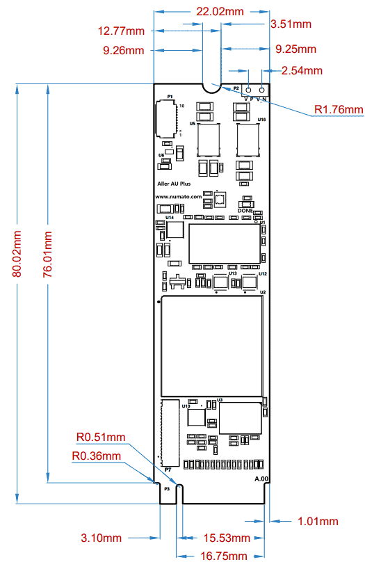
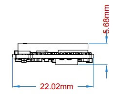
Mechanical Dimensions
Help Guide Powered by Documentor Aller AU-Plus FPGA Board with M.2 Interface
0 views April 7, 2025 megha-m 0
