Callisto K7 USB 3.1 FPGA Module
SKU: NLFX1002


Request For QuoteWanna Customize? Drop Us A Line!
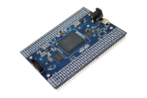
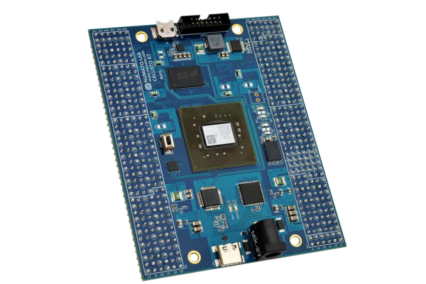
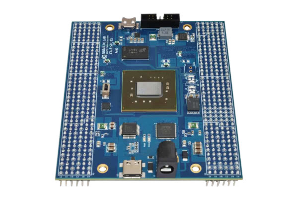
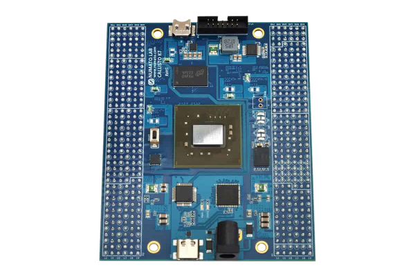
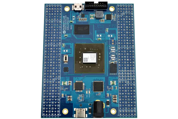
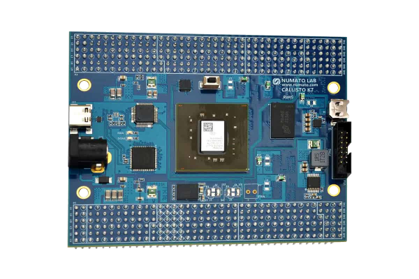
Callisto K7 is an easy-to-use FPGA Module featuring the AMD Kintex 7 FPGA with 4Gb DDR3 SDRAM. This board contains the AMD XC7K410T– FBG676 FPGA. The high-speed USB 3.1 interface (USB-C connector) provides a fast and easy configuration download to the onboard SPI flash. There is no need for a programmer or special downloader cable to download Bitstream to the board. The FPGA Module also provides easy access to JTAG signals on a standard Xilinx Platform Cable compatible header. Callisto K7 provides the user with the flexibility of adding their own peripherals through IO Expansion Headers.
Features
- FPGA: AMD XC7K160T in FBG676 package
- DDR3: 4Gb DDR3 (MT41J256M16HA-125:K or equivalent)
- Flash memory: 512 Mb Quadbit SPI flash memory (S25FL512SDSBHV210/IS25LP512M-RHLE)
- 1 x 100MHz CMOS oscillator
- USB 3.1 Gen1 @5Gbps (USB Type-C connector)
- Onboard voltage regulators for single power rail operation
- 12V DC power supply
- A Push Button for the reset pin
- JTAG header for programming and debugging
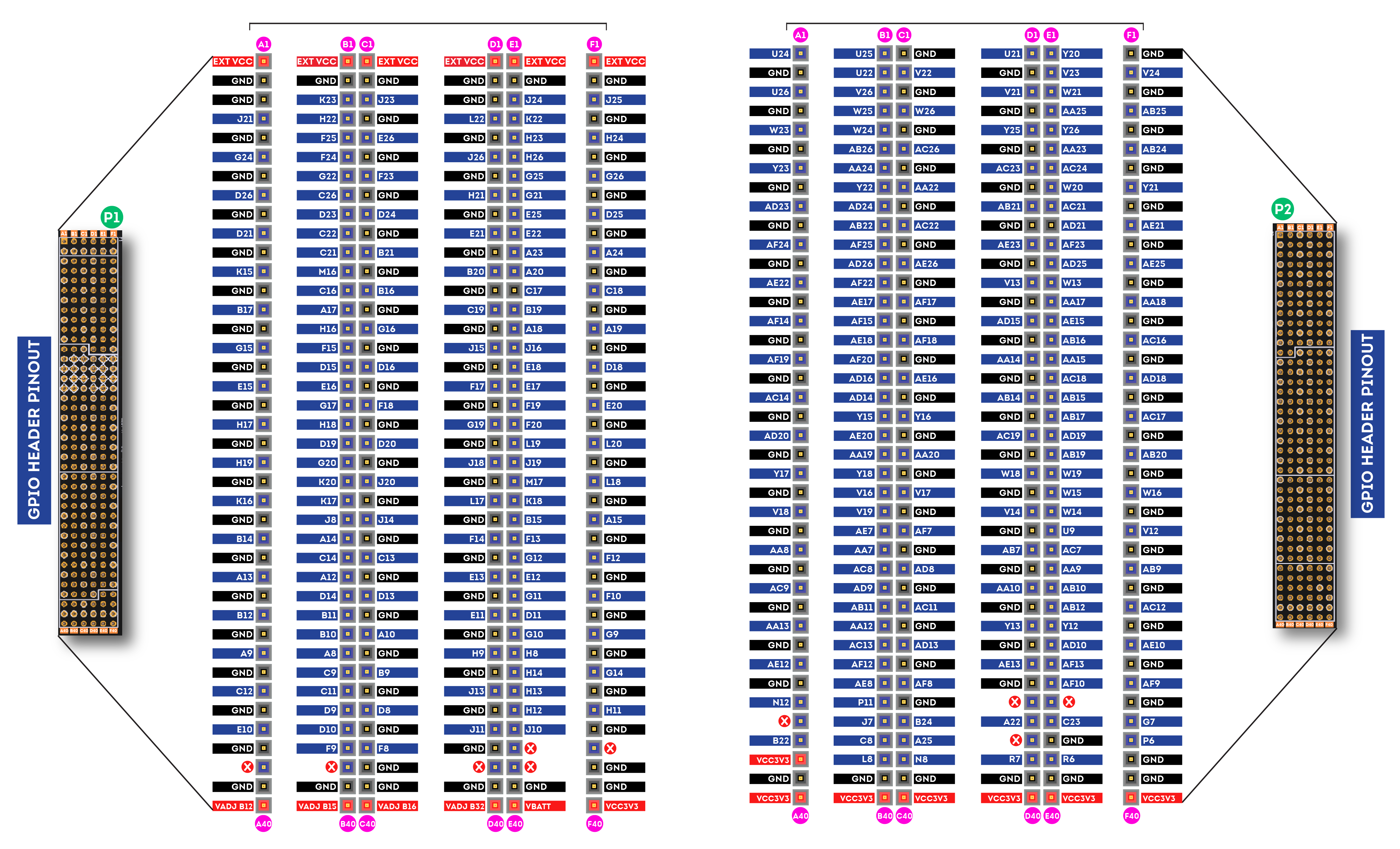
- 274 IOs for user-defined purposes
- All user IOs are length matched and can be used as differential pairs
Applications
- Product Prototype Development
- Communication Device Development
- Accelerated Computing Integration
- Development and Testing of Custom embedded processors
- Signal Processing
- Educational tool for Schools and Universities
Specifications
| Attribute | Value |
|---|---|
| Weight | 0.8 lbs |
| Dimensions | 6 × 4 × 1 in |
| FPGA | |
| Memory | |
| Number Of GPIOs (Max) | |
| Configuration Options | |
| Non-Volatile Configuration Storage | S25FL512SDSBHV210 |
| Number of Clock Sources | 1 |
| Communication | USB 3.1 |
| Primary Clock Frequency | |
| Shipping Hardware | V2 |
| HTS | 8542.39.0001 |
| ECCN | 3A991.d |
Related products